-
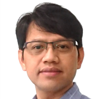 Agus SubagyoFaculty of Information Science and Technology
Associate ProfessorResearch Layer- Materials Creation
- Process
- Device
Keyword- Low-dimensional materials
- Half-metallic materials
- Nanoelectronics/ spintronics device
- Surface atomic structure/spin state measurement
Keyword- Low-dimensional materials
- Half-metallic materials
- Nanoelectronics/ spintronics device
- Surface atomic structure/spin state measurement
-
 Eiji HattaFaculty of Information Science and Technology
Assistant ProfessorResearch Layer- Materials Creation
- Process
Keyword- Monolayers
- Hierarchical structure growth
- Nanoscale and microscale structure analysis
- Novel expression dynamics exploration
Keyword- Monolayers
- Hierarchical structure growth
- Nanoscale and microscale structure analysis
- Novel expression dynamics exploration
-
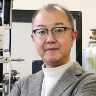 Hiromichi OhtaResearch Institute for Electronic Science
ProfessorResearch Layer- Materials Creation
- Process
- Device
Keyword- Functional oxides
- Thermal switches
- Thermoelectric energy conversion
- Pulsed laser deposition
- Thermal conductivity
- Thermopower
Keyword- Functional oxides
- Thermal switches
- Thermoelectric energy conversion
- Pulsed laser deposition
- Thermal conductivity
- Thermopower
-
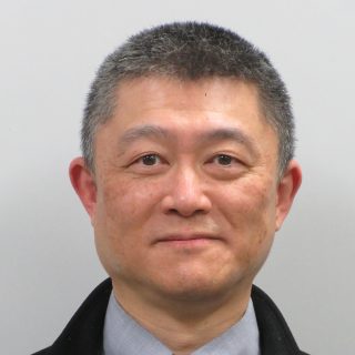 Hirotake SugawaraFaculty of Information Science and Technology
Associate ProfessorResearch Layer- Process
Keyword- modeling and simulation of plasmas
- processing plasmas for etching,thin film deposition,and surface modification
- control of plasmas by magnetic fields
Keyword- modeling and simulation of plasmas
- processing plasmas for etching,thin film deposition,and surface modification
- control of plasmas by magnetic fields
-
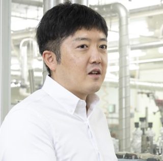 Katsuhiro TomiokaFaculty of Information Science and Technology
ProfessorResearch Layer- Materials Creation
- Process
- Device
Keyword- Semiconductor nanostructures
- Thin-film growth / epitaxy
- Semiconductor devices
- Semiconductor device process
Keyword- Semiconductor nanostructures
- Thin-film growth / epitaxy
- Semiconductor devices
- Semiconductor device process
-
 Kazuhisa SueokaFaculty of Information Science and Technology
ProfessorResearch Layer- Process
- Analysis
Keyword- Scanning probe microscopy
- Surface atomic structure measurement
- Magnetic field sensors
- Surface spin state measurement/Spin-dependent spectroscopy
- Micromagnetic field measurement
Keyword- Scanning probe microscopy
- Surface atomic structure measurement
- Magnetic field sensors
- Surface spin state measurement/Spin-dependent spectroscopy
- Micromagnetic field measurement
-
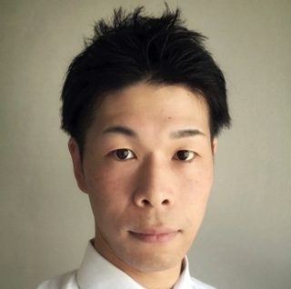 Kazuki NagashimaResearch Institute for Electronic Science
ProfessorResearch Layer- Materials Creation
- Process
- Device
- Applied Systems Creation
Keyword- Metal oxide nanowires/nanosheets
- Nano-semiconductor sensors
- Heterogeneous material integration process
- Function-combined device
- Artificial olfaction
- Surface chemical modification
- Collection and exploition of chemical information
Keyword- Metal oxide nanowires/nanosheets
- Nano-semiconductor sensors
- Heterogeneous material integration process
- Function-combined device
- Artificial olfaction
- Surface chemical modification
- Collection and exploition of chemical information
-
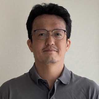 Kazumichi KobayashiFaculty of Engineering
Associate ProfessorResearch Layer- Process
Keyword- High-Knudsen number
- Knudsen diffusion
- adsorbed coefficient
- Boltzmann equation
Keyword- High-Knudsen number
- Knudsen diffusion
- adsorbed coefficient
- Boltzmann equation
-
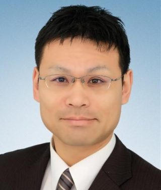 Kentaro TomitaFaculty of Engineering
Associate ProfessorResearch Layer- Process
Keyword- EUV lithography
- EUV actinic light source
- EUV light source plasma
- electron temperature
- electron density
- Thomson scattering
Keyword- EUV lithography
- EUV actinic light source
- EUV light source plasma
- electron temperature
- electron density
- Thomson scattering
-
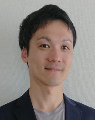 Kuniharu TakeiFaculty of Information Science and Technology
ProfessorResearch Layer- Process
- Device
- Applied Systems Creation
Keyword- Nano material devices
- Printed electronics
- Edge computing system
- Flexible MEMS
- Flexible devices
Keyword- Nano material devices
- Printed electronics
- Edge computing system
- Flexible MEMS
- Flexible devices
-
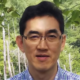 Masamichi AkazawaResearch Center For Integrated Quantum Electronics
Associate ProfessorResearch Layer- Process
- Device
Keyword- Nitride semiconductor device fabrication process
- Surface/interface control of nitride semiconductors
- Defect control of nitride semiconductors
- MOS structures
Keyword- Nitride semiconductor device fabrication process
- Surface/interface control of nitride semiconductors
- Defect control of nitride semiconductors
- MOS structures
-
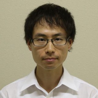 Ryuichi OhtaResearch Institute for Electronic Science
Associate ProfessorResearch Layer- Process
- Device
Keyword- Semiconductor nanofabrication
- Cryogenic microspectroscopy
- Nanophotonics
- Laser cooling
Keyword- Semiconductor nanofabrication
- Cryogenic microspectroscopy
- Nanophotonics
- Laser cooling
-
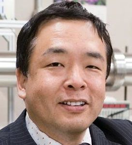 Tetsu YonezawaFaculty of Engineering
ProfessorResearch Layer- Process
Keyword- Low-temperature sintering process
- High-reliability bonding
- High fracture strength materials
- Conductive paste
- Via filling
- 3D integrated wiring technology
- Copper sintered interconnects
- High-density wiring
- Low-temperature process packaging
- Next-generation semiconductor packaging
- Copper nano-ink technology
-
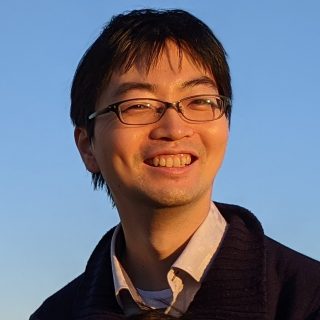 Tsukasa KatayamaResearch Institute for Electronic Science
Associate ProfessorResearch Layer- Materials Creation
- Process
- Device
Keyword- Thin film crystal growth
- Ferroelectric thin film
- Piezoelectric thin film
- Dielectric thin film
- Peeling technology
Keyword- Thin film crystal growth
- Ferroelectric thin film
- Piezoelectric thin film
- Dielectric thin film
- Peeling technology
-
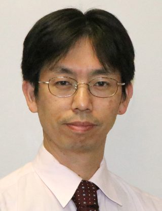 Yasutaka MatsuoResearch Institute for Electronic Science
ProfessorResearch Layer- Process
- Analysis
Keyword- Atomic Layer Deposition
- Time resolved PEEM
- Characterization of Organic/Inorganic interface
- Development of Nanoprocessing
Keyword- Atomic Layer Deposition
- Time resolved PEEM
- Characterization of Organic/Inorganic interface
- Development of Nanoprocessing
-
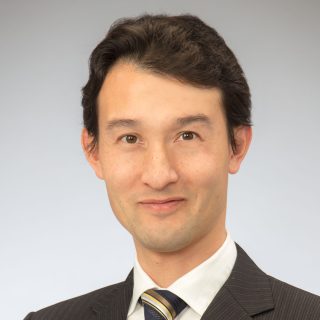 Yuki KimuraInstitute of Low Temperature Science
ProfessorResearch Layer- Process
Keyword- Electron microscopy
- in-situ observation
- wet process
- cleaning
Keyword- Electron microscopy
- in-situ observation
- wet process
- cleaning